3D printing
PCBend: flexible printed circuits for maximum creativity
Date:
Date:
Changed on 11/09/2023
In just a few years’ time, you might be reading a newspaper on a screen that folds just like real paper, watching images on a screen in the form of a ring, or lighting up your living room using a light with a futuristic design. Attendees at the upcoming edition of Siggraph, the leading conference for the world’s computer graphics community, will be given a taste of these innovative objects through a presentation of the process developed by two young researchers, Marco Freire and Manas Bhargava.
The first of the two is in the process of completing his PhD within the project team MFX - a joint undertaking involving Inria and the Laboratoire lorrain de recherche en informatique et ses applications (Loria) - while the second is a doctoral student at the Institute of Science and Technology Austria (ISTA), working within the Computer Graphics and Digital Fabrication research group headed up by Bernd Bickel. The two teams are long standing partners, having worked together on a range of projects on the subject of computer graphics and fabrication. The most recent of these, PCBend, saw the two young PhD students pooling their skills to work towards a common goal. This project emerged from ideas shared by researchers from the two teams, following on from research carried out as part of previous projects - including the ERC project Materializable on the Austrian side.
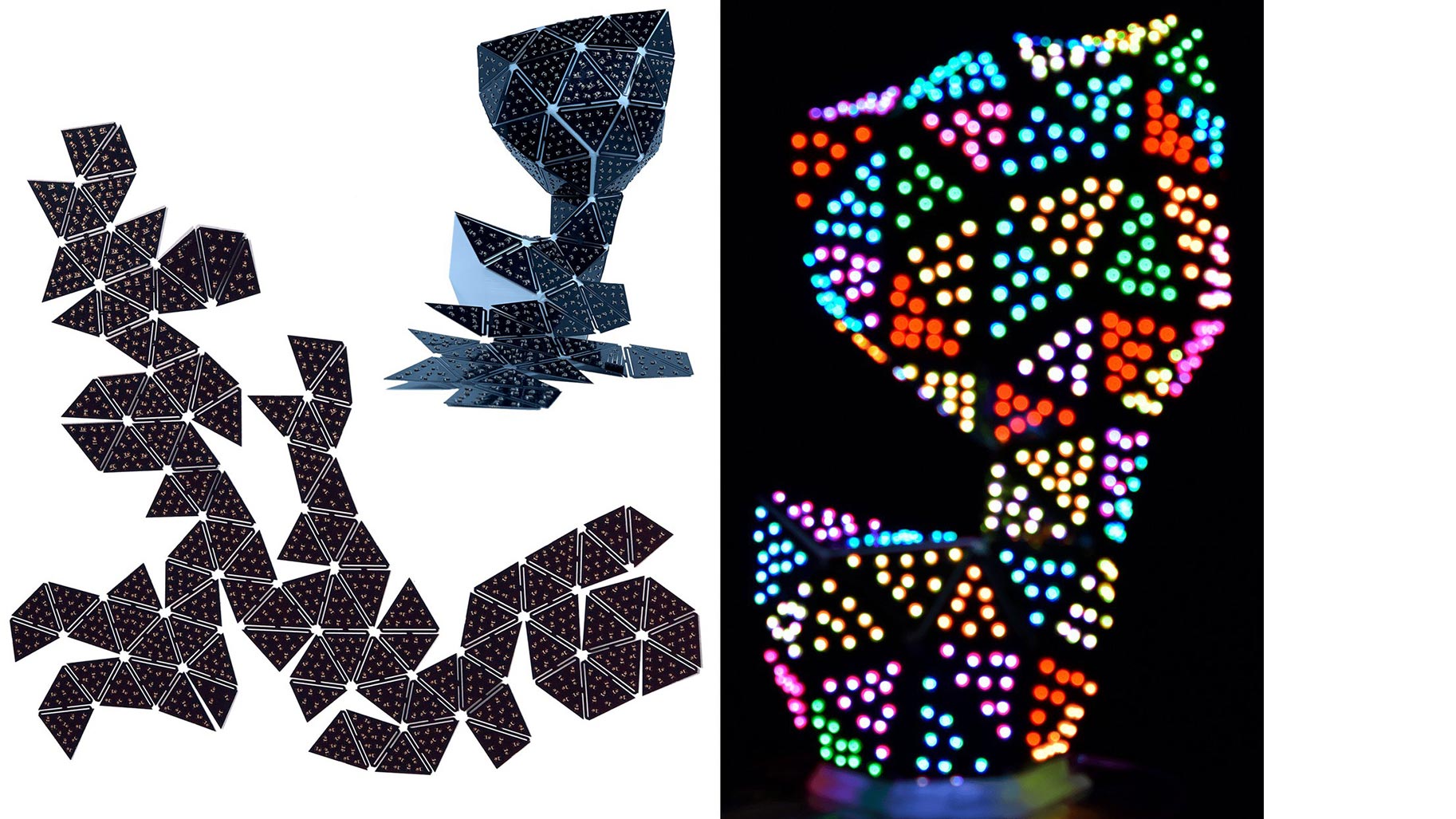
“PCBend was set up to develop a digital and computational methodology for designing electronic circuits capable of being folded onto a surface, thereby creating volumes. These circuits are then operational in 3D form, with varying degrees of complexity”, says Marco Freire. The result was a surprising electronic circuit, which the two PhD students will be presenting at the Siggraph conference using an original example: an object representing a cat fitted with light-emitting diodes (LEDs) in red, green and blue - the three colours used by our computer and television screens.
“Introducing a third dimension increases the potential for designing objects...but also raises some fascinating problems on the mathematical and computing side of things”, says Manas Bhargava. The process developed by the two researchers comprises different steps, the shape of the volume obtained by folding an initial surface containing printed circuit boards. Unlike paper, these circuit boards break when bent beyond a certain angle. The final surface, comprised of PCB panels onto which the electronic components are soldered, features cutting patterns enabling it to be folded.
“The algorithm designed for PCBend designs plans for printed circuit boards in a fully automated way. It incorporates all of the stages for optimising the geometry of PCB panels with a view towards folding, before optimising the circuit and the wiring for the LEDs on the surface as well”, explains Marco Freire.
To give you an idea of how impressive this is, consider the complexity of origami: although it is easy to get simple volumes from elementary surfaces (three triangles deployed around a central triangle can be folded into a pyramid, for example), this is much harder for more elaborate volumes. “We developed a special algorithm for determining which 2D shape will enable us to arrive at the desired 3D shape. What it does is split this complex problem into a number of easier problems, defined by an arrangement of triangles. Each of these sub-problems is then solved individually”, explains Manas Bhargava. Once produced, the electronic circuits can then be folded and glued onto a printed 3D surface: as simple as that!
The advantage of this process is that it uses only standard materials and procedures, thereby reducing manufacturing costs and time frames. What’s more, there is no need for any advanced scientific knowledge or highly specialist technical skills. “MFX set itself the target of designing technology that would be accessible to as many people as possible: we developed our algorithms in an open-source environment, and we will be sharing them with the scientific community and anyone else interested in designing new objects”, says Marco Freire.
What does the team have its sights set on now? The current algorithm will need to be improved in order to enable more complex geometries. Another challenge is increasing the LED density further, either using smaller LEDs, or finding ways to pack them even tighter.
Looking forward, what industrial applications might be possible? “Curved surfaces are of interest to automobile and urban design manufacturers. More broadly, from robotics and architecture to electronics and mass-market digital technology, there are a whole host of ways in which the process developed through PCBend could be used”, say Manas Bhargava and Marco Freire. The future is looking bright.
Suitable for all:
Research paper: